|


  | 
 Introduction Introduction
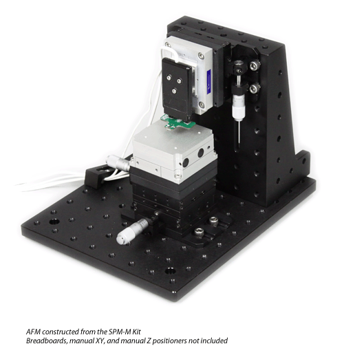
 The SPM-M Kit combines the MadPLL® instrument package with Mad City Labs high resolution nanpositioning systems to form a high performance, closed loop, scanning Akiyama probe or tuning fork AFM. The seamless integration of hardware combined with the built-in automated control of MadPLL® means that you can concentrate on getting results, not tweaking parameters. Applications for the SPM-M Kit include nanoscale characterization and nanoscale fabrication applications such as optical antennas, nano-optics, semiconductors, data storage, and more. The SPM-M Kit is ideal for research and teaching laboratories offering high performance, versatility, simplicity and excellent value. The SPM-M Kit combines the MadPLL® instrument package with Mad City Labs high resolution nanpositioning systems to form a high performance, closed loop, scanning Akiyama probe or tuning fork AFM. The seamless integration of hardware combined with the built-in automated control of MadPLL® means that you can concentrate on getting results, not tweaking parameters. Applications for the SPM-M Kit include nanoscale characterization and nanoscale fabrication applications such as optical antennas, nano-optics, semiconductors, data storage, and more. The SPM-M Kit is ideal for research and teaching laboratories offering high performance, versatility, simplicity and excellent value.
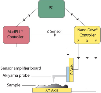
At left: Schematic of a typical AFM instrument based on the SPM-M Kit. |
| The SPM-M Kit includes:
|
- 3 axis closed loop Nano-Drive® controller
- Z axis open loop/close loop switch (OCL option)
- AFMView™ Software
- AFMView™ Tutorial
- Adapter plate between preamplifier and Nano-OP30
- Adapter plate to Thorlabs MT1 micropositioner
- Application note: "AFM Kit with manual positioning"
- Application note: "Tungsten tip etching station"
| |
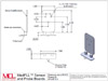
MadPLL® is a powerful instrument package that allows the user to create an inexpensive, high resolution resonant scanning probe microscope using Mad City Labs nanopositioning systems. The MadPLL® package includes a digital phase lock loop (PLL) controller, software, sensor amplifier board, and resonant probe mounting board. MadPLL® includes five (5) each of the vertical, horizontal, Akiyama, and blank probe boards. In addition, each unit is shipped with five (5) tuning forks. Additional probe boards and tuning forks can be purchased separately.
|
Available options:
- 12 in. x 12 in. x 13 in. acrylic enclosure
- LED illuminator
- Motorized Z-axis approach
- Manual micropositioning stages for XY, Z manipulation
- Breadboard
- L-Bracket
- Fasteners or clamps
|
Recommended additional items:
- Vibration isolation table
| |
Absolute Metrology
The SPM-M Kit incorporates the Nano-SPM200 and Nano-OP30 with a three axis Nano-Drive® controller for closed loop nanopositioning in X, Y, and Z. These systems incoporate Mad City Lab's proprietary PicoQ ® sensor technology for closed loop feedback control, offering significant advantages in terms of image quality, accuracy and repeatability over open loop scanners. The sensor signal from all three axes can be read during AFM scans via the analog output signal or USB, thus minimizing the effects of hysteresis, curvilinear motion, and creep that result if data are analyzed using assumed commanded positions. Using position information from closed loop sensors also eliminates the need to scan a calibration grid in XYZ before scanning every sample. Scanning with closed loop nanopositioners saves time and improves image quality. Closed loop feedback also allows the nanopositioners to move and return to commanded positions with much more reliability than open loop systems, allowing users to return to previously scanned features for further analysis. For further information about the PicoQ ® sensors used in Mad City Labs nanopositioning systems, see our Technical Information pages on high resolution sensors and nanopositioning accuracy. |
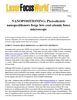
AFM Video Tutorial
Instant AFM - just add science!The video at the page linked below illustrates how to use the SPM-M kit along with an Akiyama Probe, manual coarse positioners, and hardware to create a low cost, easy assembly, high resolution AFM.
|
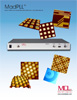
Image Gallery
Seeing is Believing!The images below were acquired using similar configurations to the SPM-M Kit.
 |
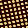
Calibration grid
(100nm tall lines, 2µm apart)
10µm x 10µm
Unidirectional scan
Self oscillation mode, constant probe signal
Z force feedback: frequency
Data taken using MadPLL® with Nano-HS3 3-axis nanopositioning system. |
 |
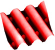
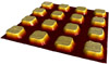
Calibration grid
(100nm tall pegs, spaced 2µm apart)
10µm x 10µm
Unidirectional scan
Self oscillation mode, constant probe signal
Z force feedback: frequency
Data taken using MadPLL® with Nano-HS3 3-axis nanopositioning system. |
 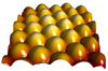 |
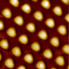
Fly eye
100µm x 100µm
Bidirectional scan
PLL mode, constant probe signal
Z force feedback: frequency
Data taken using MadPLL® with Nano-OP30 nanopositioning system (Z-axis), Nano-OP100 nanopositioning system (XY axes) |
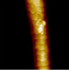 |
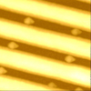
Human hair
100µm x 100µm
Bidirectional scan
Self oscillation mode, constant probe signal
Z force feedback: frequency
Data taken using MadPLL® with Nano-OP30 nanopositioning system (Z-axis), Nano-OP100 nanopositioning system (XY axes) |
  |
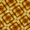
PMMA pattern, uncured
10 µm x 10 µm
Bidirectional scan
Self oscillation mode, constant probe signal
Z force feedback: frequency
Data taken using MadPLL® with Nano-OP30 nanopositioning system (Z-axis), Nano-OP100 nanopositioning system (XY axes) |
 |
Integrated circuit
100 µm x 100 µm
Bidirectional scan
Self oscillation mode, constant probe signal
Z force feedback: frequency
Data taken using MadPLL® with Nano-OP30 nanopositioning system (Z-zxis), Nano-OP100 nanopositioning system (XY axes) |
  |
Calibration grid
40 µm x 40 µm
Unidirectional scan
Self oscillation mode, constant probe signal
Z force feedback: frequency
Data taken using MadPLL® with Nano-OP30 nanopositioning system (Z-zxis), Nano-OP100 nanopositioning system (XY axes) |
 |
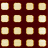
Calibration grid
(100nm tall, 10µm pitch)
70 µm x 70 µm
Unidirectional scan
PLL mode, constant probe signal
Z force feedback: frequency
Data taken using MadPLL® with Nano-OP30 nanopositioning system (Z-axis), Nano-OP100 nanopositioning system (XY axes) |
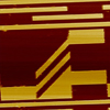 |
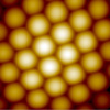
Etched structures
80 µm x 80 µm
Bidirectional scan
Self oscillation mode, constant probe signal
Z force feedback: frequency
Data taken using MadPLL® with Nano-OP30 nanopositioning system (Z-axis), Nano-OP100 nanopositioning system (XY axes) | |
Tungsten Tip Etching
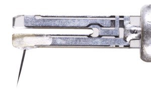 An etched tungsten tip glued to a quartz tuning fork. An etched tungsten tip glued to a quartz tuning fork.One way to produce sharp probe tips suitable for building an AFM is to electrochemically etch tungsten wire. This method can produce a tip radius of better than 50nm. Post etching techniques can even sharpen the tip down to a <1nm tip radius. These sharp tungsten tips can be mounted to quartz tuning forks for AFM or for other types of scanning probe microscopy like scanning tunneling microscopy (STM). There are a variety of methods to choose from to etch the tungsten wire. The single lamella technique is easy to setup and can consistently produce sharp tips. Among the requirements for this process are a metallic ring, a beaker, Potassium Hydroxide (KOH), tungsten wire, and a voltage source. A drop of KOH is added to the metal ring suspended above the beaker, forming a thin film or lamella of KOH inside the metallic ring. The negative terminal of the voltage source is then connected to the suspended metallic ring. This will form the negative electrode. The beaker below the ring is then filled with KOH and the positive terminal of the voltage source is wired into the KOH solution. This forms the positive electrode. The tungsten wire is then dipped through the center of the lamella and into the KOH in the beaker. The voltage source is then turned on which begins the etching process. The tungsten is electrochemically etched at the lamella. The etching process automatically stops when the tungsten wire is etched so thin that the portion of wire below the lamella falls off and drops into the beaker. The remaining tungsten wire above the lamella is removed and any remaining KOH or contaminants are rinsed off with distilled water. This leaves a very sharp tip suitable for use in AFM or other types of SPM. See the Application Note: "Tungsten Tip Etching Station" for further information. |
|
|
phone: 608.298.0855 fax: 608.298.9525
Copyright © 2014 | | |
 公司新闻
公司新闻


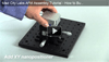
 Mad City Labs AFM Assembly Tutorial - How to Build an "Instant" Atomic Force Microscope