
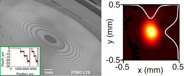
 Focusing of 4.75 Thz (λ = 63 µm) radiation with laser fabricated Fresnel lens Focusing of 4.75 Thz (λ = 63 µm) radiation with laser fabricated Fresnel lens
THz imaging in an emerging technology in astronomy, medicine, art conservation, security, materials inspection, etc. Off-axis parabolic mirrors and refractive lenses are available commercially and very often are employed in THz imaging setups. In order to reduce the complexity of the THz systems and make them more compact, diffractive lenses such as multilevel phase Fresnel lenses and Fibonacci lenses have been developed on high-resistivity silicon and in metal. High repetition rate ultrashort (1 MHz, 10 ps, 1064 nm)picosecond laser pulses were used to fabricate Fresnel lenses in silicon. Depending on the lens design, laser beam scanning with both galvanometric and polygon scanners were utilised. In batch processing with a polygon scanner, material removal rate up to 1.46 mm3/s was achieved. Using this technology, silicon Fresnel lenses for various THz frequencies, including 0.6 Thz and 4.75 Thz, were fabricated. High focusing performance with a focal spot diameter of only 2.4 times larger than the wavelength was achieved. In general, with this technology, optical components for the 0.1 – 5 THz frequency range can be manufactured. The aperture of the optical element ranges from 10 to 25 mm.
Fibonacci terahertz imaging by silicon diffractive optics
Related products: Atlantic series
Laser processing for precise fabrication of the THz optics
Related products: Atlantic series
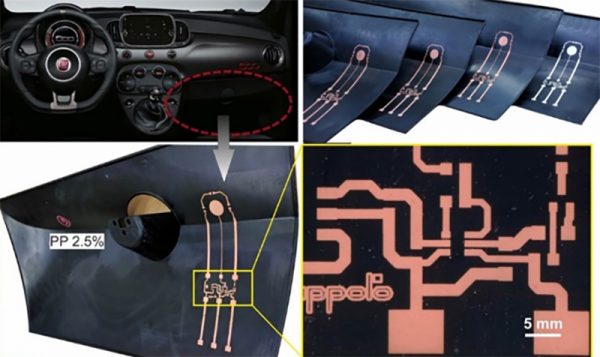 Electronic circuit traces of capacitive touch button for Fiat 500 gloves box cover. Fabricated using SSAIL technology Electronic circuit traces of capacitive touch button for Fiat 500 gloves box cover. Fabricated using SSAIL technology
Fabrication of circuit traces is the most challenging task in Moulded interconnect devices (MID) production, being both technically difficult to achieve and difficult to make cost effectively. Moulded interconnect devices (MID) – an injection-moulded thermoplastic part with integrated electronics – offer material, weight and cost savings by integrating electronic circuits directly into polymeric components. Selective Surface Activation Induced by Laser (SSAIL) is a new technology for writing electronic circuits directly onto the dielectric material. This is done by modifying the surface properties with a picosecond pulse laser and has been developed at the Center for physical sciences and technology. Picosecond lasers can write the circuits directly by modifying the surface of polymers followed by an electroless metal plating. SSAIL is a three-step process. First is surface modification by laser; second is chemical activation of the modified areas; and the last step is metal deposition by electroless plating. The new technology offers laser writing speeds of up to 4m/s, and therefore spatial plating pitch is kept narrow at 25 µm.
Laser-assisted selective copper deposition on commercial PA6 by catalytic electroless plating – process and activation mechanism
Related products: Atlantic series
Laser-induced selective copper plating of polypropylene surface
Related products: Atlantic series
Colour-difference measurement method for evaluation of quality of electrolessly deposited copper on polymer after laser-induced selective activation
Related products: Atlantic series
Photopolymerization is a powerful and versatile light-activated resin solidification process. It is attractive for the fabrication of complex micrometer-size three-dimensional (3D) structures by employing nanosecond as well as picosecond lasers. Many fabrication techniques of polymeric microstructures are based on photopolymerization via photolithography, digital light processing lithography, rapid prototyping, multi-photon polymerization, 3D printing, interference lithography, etc. Polymeric microstructures with a prescribed shape and thickness are desirable for a wide range of applications: tissue engineering, electronics and optics, coating, adhesives, drug delivery, microfluidics and surface science.
Source: E. Stankevičius, E. Daugnoraitė, etc. Mechanism of pillars formation using four-beam interference lithography. Optics and Lasers in Engineering 116, 41-46 (2019).
Thermal control of SZ2080 photopolymerization in four-beam interference lithography
Related products: Atlantic series
Mechanism of pillars formation using four-beam interference lithography
Related products: Atlantic series
 ITO electrode modified with gold nanoparticles ITO electrode modified with gold nanoparticles
ITO electrodes modified with gold nanoparticles possess faster electron transfer rates and larger current responses than bare ITO electrodes. Therefore such electrodes could be applied for the creation of highly sensitive and selective future sensors. The generation of gold nanoparticles on ITO electrodes using nanosecond lasers has advantages over drop-casting deposition as they do not use colloidal solutions and the generation of gold nanoparticles occurs directly on the desired surface. The main advantages of nanosecond laser processing are submicron treatment accuracy, low thermal impact to the substrate and surrounding areas and selective generation of nanoparticles on desired place and shape of the surface.
Source: E. Stankevičius, M. Garliauskas, etc. Engineering electrochemical sensors using nanosecond laser treatment of thin gold film on ITO glass. Electrochimica Acta 297, 511-522 (2019).
Engineering electrochemical sensors using nanosecond laser treatment of thin gold film on ITO glass
Related products: NL230 series
Germanium Sub-Microspheres Synthesized by Picosecond Pulsed Laser Melting in Liquids: Educt Size Effects
Related products: Atlantic series
Solvent-surface interactions control the phase structure in laser-generated iron-gold core-shell nanoparticles
Related products: Atlantic series
 P3 Type 2 scribe P3 Type 2 scribe
Climate and environmental concerns led to the rapid growth of renewable power generation. It is forecasted that in the near future, solar photovoltaics (PV) will become one of the major energy sources. Such demand for PV electricity could be satisfied by low cost, low material consuming thin-film devices such as copper indium gallium (di)selenide (CIGS) modules.
Lasers are extensively used in the production lines of flexible CIGS PV for all processing steps, namely P1, P2, and P3 laser scribes (with P3 being the most difficult) to produce monolithic series interconnects between cells.
However, scaling up the manufacturing throughput to several m/s or more is one of the major objectives for the successful development of CIGS thin-film technologies and the implementation of lasers into industrial production lines as a standard tool.
A modern ultrafast industrial Atlantic series laser, offering high average power at the laser pulse repetition rate of 1 MHz, showed outstanding results in scaling up the throughput of P3 Type 2 scribing in a fully functional CIGS solar cell. High pulse repetition rate enabled the P3 scribing speed of 50 m/s. The laser-induced conductivity of P3 Type 2 scribes was extremely low, ensuring minimum solar module efficiency losses. Furthermore, channels were cleanly exposed, with insignificant melting of the CIGS absorber layer and were highly repeatable.
Source: P. Gečys, E. Markauskas, etc. CIGS thin-film solar module processing: case of high-speed laser scribing. Scientific Reports. 7, 40502 (2017)
Picosecond Laser Modification of CIGS Active Layer
Related products: Atlantic series
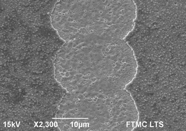
 The scanning microscope image of direct laser interference patterning example The scanning microscope image of direct laser interference patterning example
A number of applications, such as fabrication of plasmonic devices, control of surface wettability or reflectance requires a fast and reliable microstructuring approach. To produce fine periodic microstructures with lasers, Direct Laser Interference Patterning (DLIP) can be used. Interference patterning allows the distribution of laser energy over large areas and produces subwavelength features in this area with a single exposition. As if patterning was done with thousands of very tightly focused laser spots. The main drawback of this method is the limited variety of available pattern shapes. Therefore, a confocal six-beam interference optical module with polarization control for each separate beam was developed. The DLIP method works most efficiently with high pulse energy lasers. Furthermore, for precise patterning, shorter pulse duration has to be selected to avoid material melting due to thermal diffusion between the high intensity interference spots. Therefore, a high pulse energy sub-nanosecond laser (1 kHz, 300 ps, 532 nm) was used to provide high quality patterning with a relatively simple and inexpensive laser source. Using this approach, a number of patterns were obtained experimentally for the first time using the interference patterning technique. Patterning rate up to 1 m2/h was available.
Source: M. Gedvilas, S. Indrišiūnas, etc. Nanoscale thermal diffusion during the laser interference ablation using femto-, pico-, and nanosecond pulses in silicon. Phys. Chem. Chem. Phys., 2018, 20, 12166-12174.
Nanoscale thermal diffusion during the laser interference ablation using femto-, pico-, and nanosecond pulses in silicon
Related products: Atlantic series Atlantic 5 series
Fluorescence Microscopy Study of CdS quantum dots Obtained by Laser Irradiation from a Single Source Precursor in Polymeric Film
Related products: Atlantic series
In situ formation and photo patterning of emissive quantum dots in organic small molecules
Related products: Atlantic series
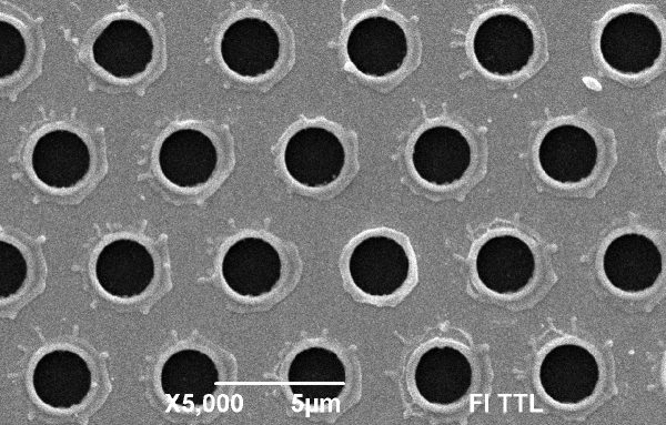
 Scanning electron microscope micrograph of thin metal film removed by direct laser writing Scanning electron microscope micrograph of thin metal film removed by direct laser writing
Metal films on glass are widely used in industry and science and cover diverse applications. Chromium film on glass is an important material in photo mask production for lithography, as well as in the production of diffraction gratings and linear optical encoders for metrology. Aluminum and silver are used as mirrors, titanium for diffractive optical elements and gold films are widely applied in biomedicine as a substrate for bio-chip production. Lasers are frequently applied for patterning metal film instead of wet chemical or plasma etching. When performing micromachining using lasers, multiple bursts of lower-power irradiation are employed to minimize heating. Metal thin films are ablated without damaging the glass substrate using nanosecond, picosecond and femtosecond laser pulses. Film thickness and drawing shape can be controlled depending on the application.
Source: V.P. Veiko, R.A. Zakoldaev, etc. Thermochemical writing with high spatial resolution on Ti films utilising picosecond laser. Optical Materials Express 9, 2729-2737 (2019).
Compact diffractive optics for THz imaging
Related products: Atlantic series
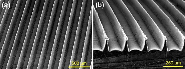 Top view (a) and cross-sectional (b) scanning electron microscope micrographs of laser ablated shark-skin-like riblet structures on pre-heated Teflon Top view (a) and cross-sectional (b) scanning electron microscope micrographs of laser ablated shark-skin-like riblet structures on pre-heated Teflon
Bio-inspired surfaces decrease friction with gases and the most recognizable textures are shark-skin-like riblets. Such surfaces can be formed using direct laser ablation with high flexibility options. The bio-inspired riblet surfaces were formed using picosecond ultraviolet laser ablation on pre-heated Teflon at various sample temperatures. The ablation of hot Teflon was found to be 30% more efficient than the conventional laser structuring at room temperature. The functional properties and surface morphologies of the laser-fabricated textures were found to be close to the simplified geometry of shark-skin. The friction of structured Teflon surfaces with the flowing air was investigated using a drag measurement setup.
Source: A. Žemaitis, J. Mikšys, etc. High-efficiency laser fabrication of drag reducing riblet surfaces on pre-heated Teflon. Materials Research Express 6, 065309 (2019).
Picosecond Pulsed Laser Ablation for the Surface Preparation of Epoxy Composites
Related products: Atlantic series
Laser processing for precise fabrication of the THz optics
Related products: Atlantic series
Solvent-surface interactions control the phase structure in laser-generated iron-gold core-shell nanoparticles
Related products: Atlantic series
Layered Seed-Growth of AgGe Football-like Microspheres via Precursor-Free Picosecond Laser Synthesis in Water
Related products: Atlantic series
Irradiation of Diamond-Like Carbon Films by Picosecond Laser Pulses
Related products: Atlantic series
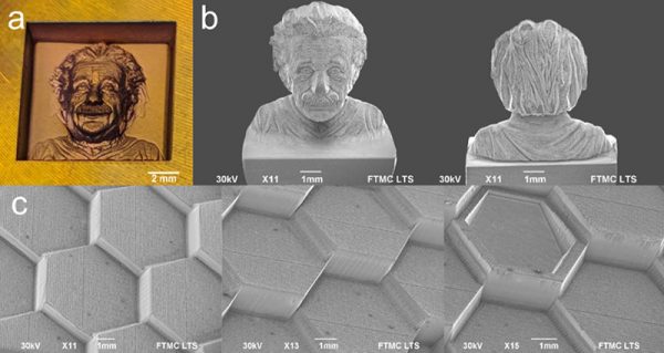 Examples of 3D laser milling Examples of 3D laser millingThe high interest of scientific and industrial societies in additive manufacturing has shown that fabrication of three-dimensional (3D) objects is needed. Mostly, 3D printing technology is based on matter melting and solidification, which changes the physical properties of the material, giving an undesirable layer-by-layer appearance, and void formation. The opposite technology to additive is subtractive manufacturing, where ultrashort pulse laser ablation can be utilised. The ultrafast lasers are the number one choice for laser milling technology due to confined laser-matter interaction during very short pulse duration. Minimal heat affected zone and melt-free treatment are achieved with ultrashort pulse lasers leading to advanced processing precision. To form a 3D object, with the help of laser pulses, the unwanted material has to be removed layer-by-layer . For this, the 3D stereolithographic file is divided into the required number of slices along the z-axis. Ultrashort pulse lasers ensure rapid micro-machining and high quality, which are the most important characteristics for industry-orientated applications.
Source: A. Žemaitis, M. Gaidys, etc. Rapid high-quality 3D micro-machining by optimised efficient ultrashort laser ablation. Optics and Lasers in Engineering 114 (2019) 83–89.
Picosecond Pulsed Laser Ablation for the Surface Preparation of Epoxy Composites
Related products: Atlantic series
Laser processing for precise fabrication of the THz optics
Related products: Atlantic series
Solvent-surface interactions control the phase structure in laser-generated iron-gold core-shell nanoparticles
Related products: Atlantic series
Layered Seed-Growth of AgGe Football-like Microspheres via Precursor-Free Picosecond Laser Synthesis in Water
Related products: Atlantic series
Irradiation of Diamond-Like Carbon Films by Picosecond Laser Pulses
Related products: Atlantic series
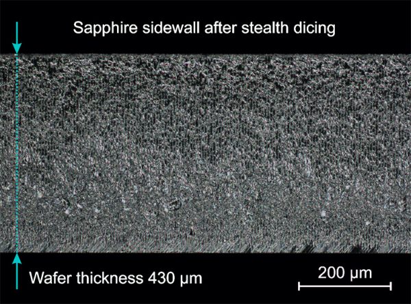
Single crystal sapphire offers superior physical, chemical, and optical properties, which make it an excellent material for wide range of applications. However, the high cost of sapphire machining precludes its use in all but the highest value applications. Stealth dicing technique using Atlantic series picosecond industrial laser is a solution that ensures the best quality and cost minimization. Using this method, ultrafast laserinduced modifications are created inside the volume of sapphire without damaging the top and bottom surfaces of the substrate, even in thick wafers. The modifications create a crack plane and sapphire is cleaved by applying external force, resulting in a clean process with almost no material loses because of effectively zero kerf width. Some applications include: high-speed integrated circuit chips, thin-film GaN-based light emitting diode substrates, wristwatch crystals and movement bearings, scratch resistant display and camera covers, and high durability optical windows for extreme applications.
Multi-photon absorption enhancement by dual-wavelength double-pulse laser irradiation for efficient dicing of sapphire wafers
Related products: Atlantic series
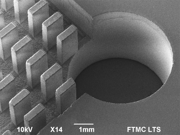 Laser milling Laser milling
The glass is an important engineering material for a number of different applications. Laser machining of transparent materials, such as flat glass, is a fast growing market, driven by new developments in displays, optoelectronics and medical device technology. Conventional glass processing techniques such as diamond drilling and dicing, water-jet drilling, sand blasting or ultrasonic processing are still commonly used in mass production, although limitations of these techniques in flexibility, processing speed and quality require a search for novel technological solutions. Laser-based techniques such as rear side glass processing can offer high quality and throughput, which can be used for glass drilling, cutting and milling applications. Typical kerf widths with such technique can be extremely reduced compared to mechanical diamond tool processing. Therefore, laser milled feature sizes can be reduced to 150 µm. Furthermore, laser cuts are taper–less, therefore, extremely high aspect ratio features can be fabricated. Glass surface chipping during processing is another important issue. However, laser-based processing with Atlantic series picosecond laser can maintain high throughput with the highest processing quality keeping surface chipping bellow 100 µm.
- Materials: soda lime glass (SLG), fused silica, BK7 glass, borosilicate glass;
- Quality: Surface chipping <100 µm, sidewall roughness <2 µm;
- Cutting throughput: 0.6 m/min (1 mm SLG glass), 0.12 m/min (5 mm SLG glass);
- Via drilling Ø 0.2-1 mm: 1 s/via (1 mm SLG), 5 s/via (5 mm SLG);
- Material removal rate: 90 mm3/min.
|
 公司新闻
公司新闻


